Design Week 6: 2/14-2/21
- John Waters
- Feb 24, 2022
- 5 min read
Updated: Mar 15, 2022
This week the team met at the west campus open lab to test the power supply prototype board.
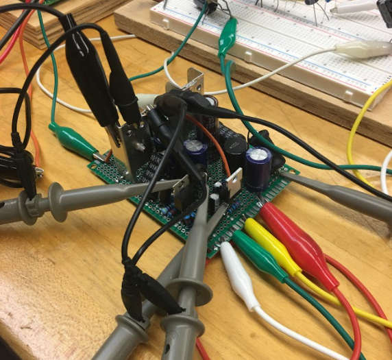
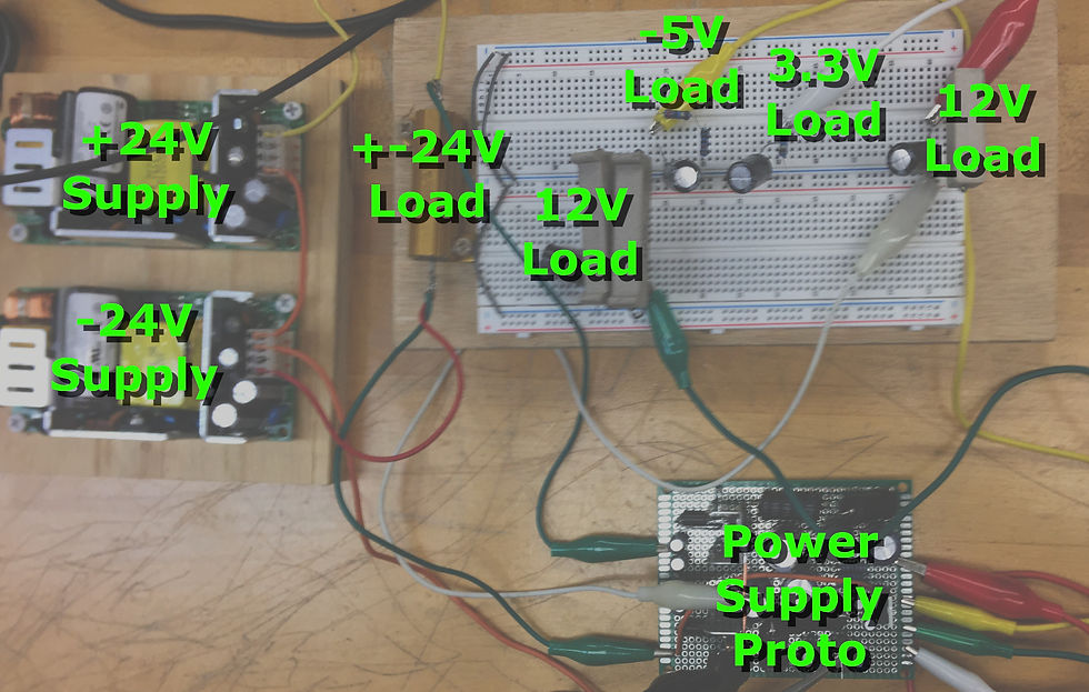
The Power Supply passed our maximum dummy-load trial!
As specified in the DER, all voltage outputs were held within 5% of the nominal value under maximum expected load conditions.
Two rounds of 20 trials were conducted. The power supply was turned on and left powered up for a total of approximately 45 minutes during testing.
The first round consisted of continuous oscilloscope measurement of all prototype board outputs. Data-points were taken from each output at 1 minute increments. The main +-24V was measured using the DMM as well. The DMM leads were placed across the entire load resistor, yielding ~48V, rather than measuring to ground for each rail of the split supply.
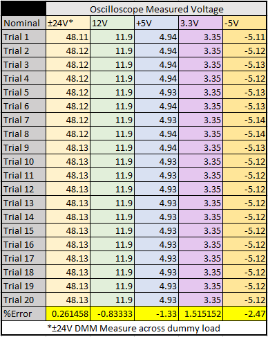
At no point did any output exceed the deviation threshold of 5%. The maximum average error was measured on the -5V rail at 2.47%.
The second round consisted of DMM measurements of each rail relative to ground (black lead of the DMM clipped to the 12V regulator heatsink) with the same 1 minute interval between measurements.

Again, all data-points fell well within the 5% benchmark. The greatest average error was again on the -5V rail at 2.01%.
Peak to Peak voltage ripple (Max Load) of each supply output was also measured. The scope channels were each set to AC coupling and vertically scaled to 50mV per division.
All supply outputs exhibited the same degree of ripple. Around 80 to 100mV peak-to-peak at the buck regulator switching frequency (52 kHz). Inexpensive bobbin inductors were used and are the likely cause of the higher-than-expected output ripple.
The LM2576 datasheet warns that the EMI generated by bobbin type inductors can induce voltage into scope probes, causing measurement errors. [1]
Regardless, this ripple can be further reduced at each device by applying filtering at supply input terminals.

Peak-to-Peak Voltage Ripple of the 12V Supply Output

Peak-to-Peak Voltage Ripple of the -5V Supply Output
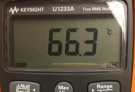
Temperature readings of each regulator were made at the end of testing to verify nothing was reaching a critical temperature under maximum current load. The highest measured temperature was 66.3 degrees Celsius on the LM237 -5V supply. This is well below the manufacture stated junction temp limit of 125 degree C. All other regulators measured within the range of 30 to 50 degrees C.

[1] Texas Instruments, "LM2576xx Series SIMPLE SWITCHER® 3-A Step-Down Voltage Regulator," SNVS107F datasheet, June 1999 [Revised May 2021]
John
Simulation of the ADC Input Buffer

2 Channel Bandpass Buffer
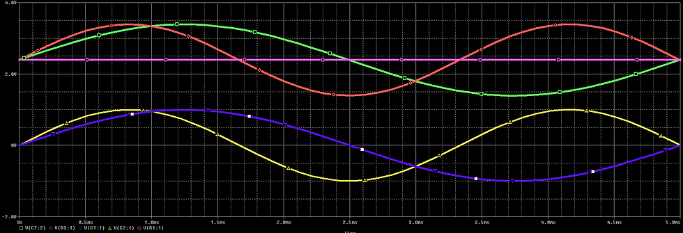
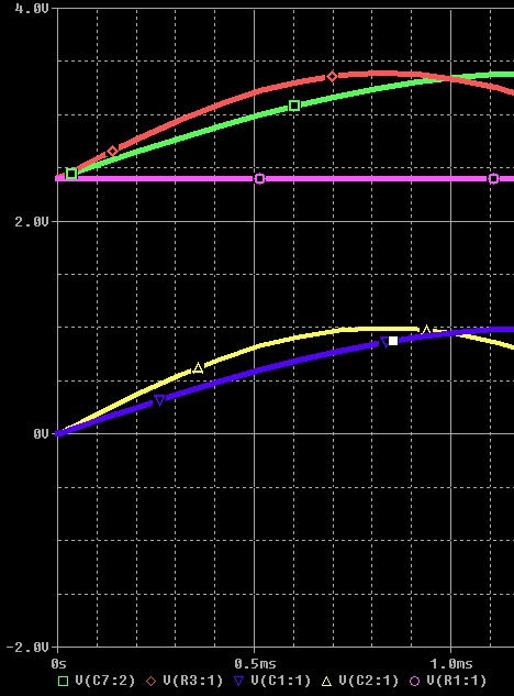

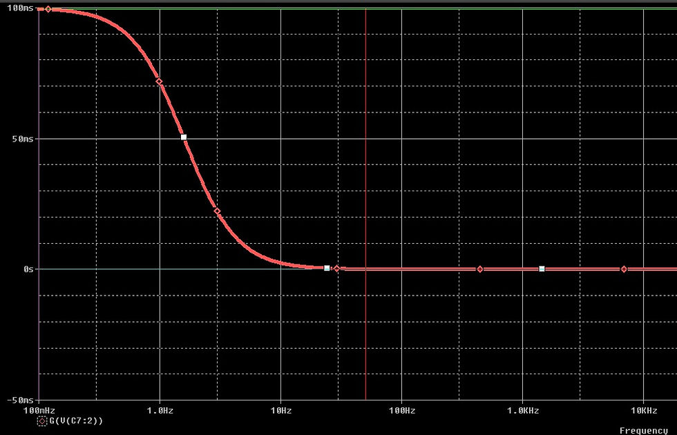

99uS of Voltage Group Delay @50Hz
In order to minimize the amount of circuitry between the mic and ADC, John combined the MIC Preamp and input buffer circuits. After further review, the 4th order LPF that was previously simulated proved to be unstable and was replaced with a 2nd order stage.


The oscillation period is roughly 2.39 - 2.19mS = 200uS or 5kHz.


The group delay dips below zero starting at around 5.5kHz. Negative group delay indicates a "predictive circuit". This is the likely cause of the instability.
Since the mic preamp already accomplishes the bandpass filtering, combining it with the buffer only requires an additional stage to apply some gain and the 2.4V offset needed for ADC input
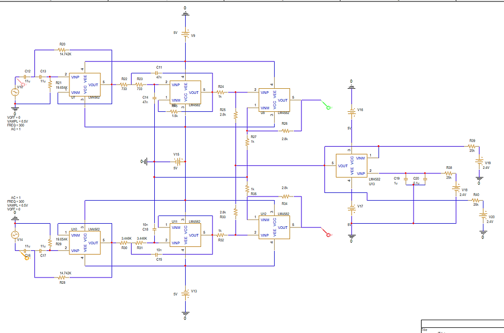
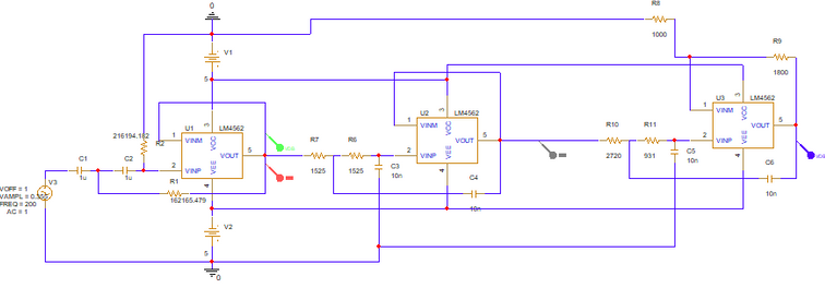
The full input stage schematic. 2 Mic Preamp and ADC Buffer Channels
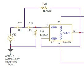
Stage 1: 2nd Order Bessel High Pass Filter fc = 1Hz. All component values calculated with OCTAVE filter design tool


Stage 2: 2nd Order Bessel Low Pass Filter fc = 3kHz
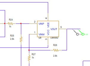
Stage 3: Non-Inverting Amp Gain 3.8 (Voltage Divider input effectively makes gain 2.8)
Designed using method in [1].

Stage 4: DC Offset Buffer (Taken from Cirrus Datasheet). [2]
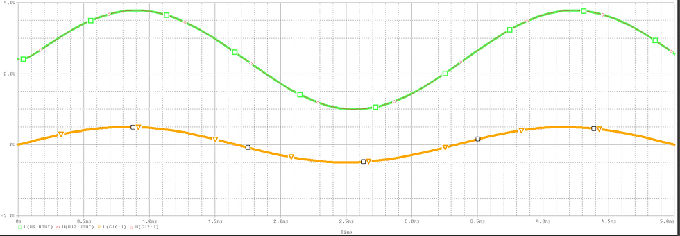
Time Domain: Output (green) is amplified and offset
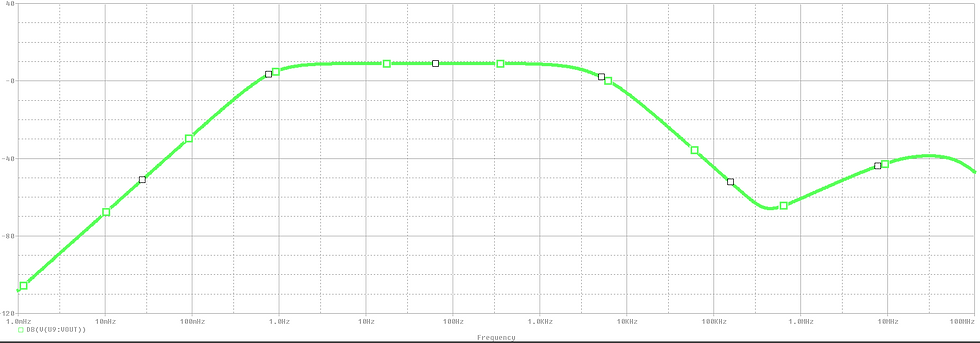
Frequency Domain Output shows expected 12dB/Octave Slopes at either end of passband. The "coming-back-up" action that starts just before 1MHz is likely due to the rising output impedance of the Op-amps, particularly the 2nd Stage one. [3]
A plain buffer using the LM4562 was used to verify


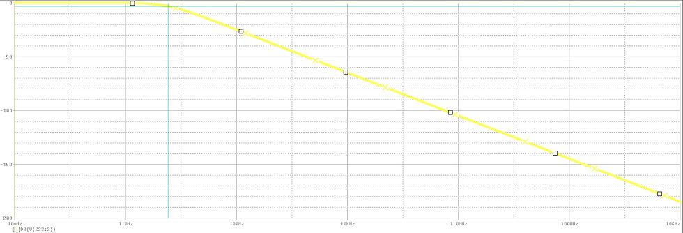
The Low Pass filter in the non-inverting input of stage 4 was also simulated verify its response
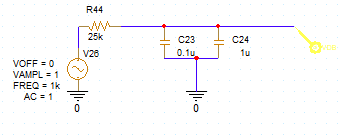
The 25k ohm resistor represents the VQ output impedance of the ADC. [2]
1/(2pi*25kohm*1.1uF)=5.78Hz

Breadboard Construction and testing will be completed next week.
[1] B, Carter, “Designing Gain and Offset in Thirty Seconds,” Texas Instruments, Dallas. TX, SLOA097, February 2002 1999
[2] Cirrus Logic, “24-Bit, 192 kHz Stereo Audio CODEC,” CS4271 datasheet, August 2005
[3] D. Self, The Design of Active Crossovers, 2nd ed. New York: Focal Press, 2018.
Hunter
The Weekly Minutes with Professor page was updated for this week, shown below.

To note, there was a mix-up with this weeks progress log not uploading (or publishing) to the website from the draft version. However, the following weeks progress log was showing, at the time, and some of this weeks assignments were accidentally added to next weeks progress log (week 7).
Pspice simulations of the DAC output and power amplifier were conducted this week.
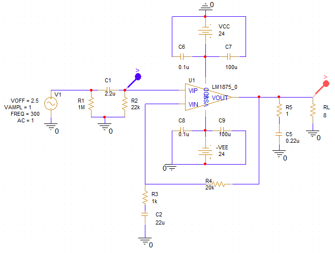
The first simulation below of the power amplifier has a feedback resistor (R4) of 20kΩ, as in the LM1875 datasheet for this schematic. This resulted in some clipping when applying an amplitude of 1.25V . This is because, it is being simulated just above the max output of the power amplifier, which can produce a 20W output into a 4 to 8Ω load. [1]
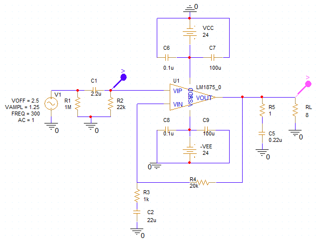
The schematic with feedback resistor (R4) at 20kΩ, shown above. The image below shows clipping in the simulation of the output load:
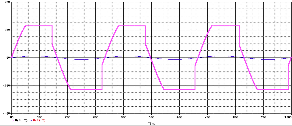
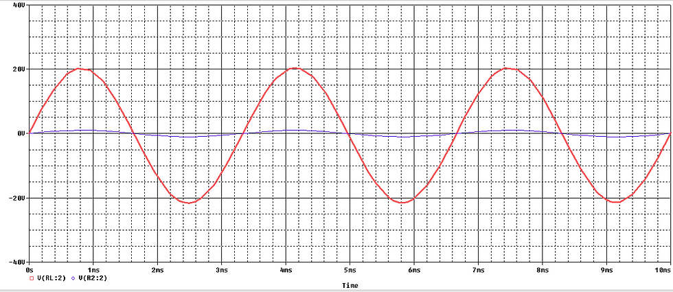
The addition of the sources 1.25V amplitude is what is causing clipping at the output. A slight modification can fix the clipping. The simulation (Below) demonstrates how changing the source's amplitude from 1.25V to 1V produces an expected max output of 20V-peak (or 14.14Vrms).
Expected max output at the load of the power amplifier is shown below:
Reducing the feedback resistor's value (R4) to 9kΩ reduces the gain to around 12Vp (or 8.48Vrms), shown below.
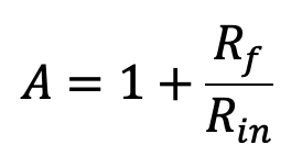
Gain for a Non-Inverting Amplifier is:
A potentiometer, of at least (10kΩ @1W), is being considered as a possible replacement of the 9kΩ feedback resistor. If a potentiometer is used as the feedback resistor this would allow us to adjust the output gain for any possible fine tuning.
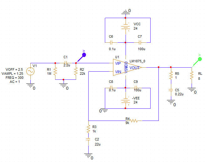
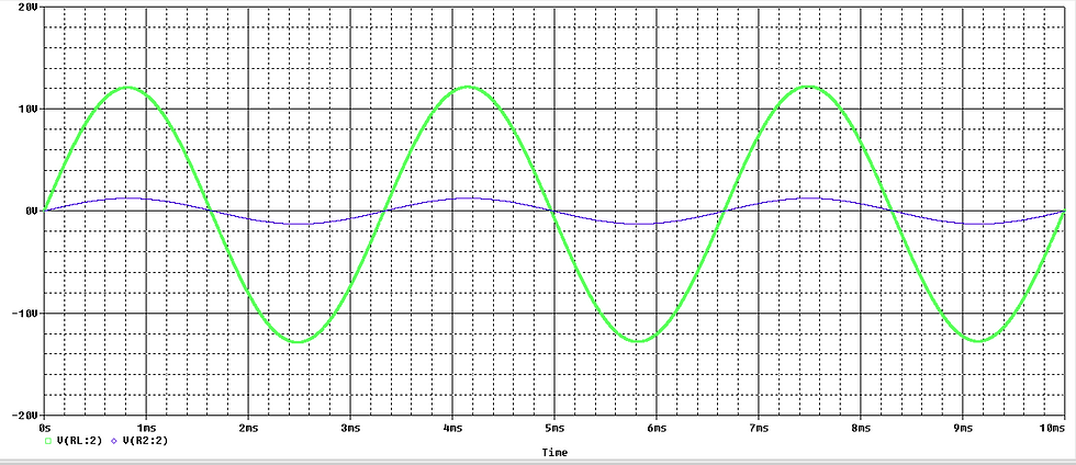
The LM1875 Power-Amplifier is typically used with 4 to 8Ω loads. The transducers that will be used in our design are both 16Ω, but if they are bridged (or connected in parallel) they become 8Ω's each, so this not a concern but will need to be verified. The simulation of the 16Ω load is shown below:

The output, shown below, with the 16Ω load applied, is identical to the simulation with the 8Ω load. These results will still be examined once the power amp is built to determine if this behavior is normal and efficient when a 16Ω load is applied.
Otherwise, the transducers will simply be bridged, to split the load, allowing each transducer to become 8Ω's each, which is within the typical load resistance in accordance to LM1875's datasheet.

References:
[1] Texas Instrument, “LM1875 20W Audio Power Amplifier,” LM1875 Ti datasheet , Dallas. TX, SNAS524A, Revised May 2004.


Comments