Design Week 7: 2/21-2/28
- Hunter Keating
- Mar 15, 2022
- 6 min read
Updated: Mar 24, 2022
This week the team continued working on the input and output stages of the device. The team met on Tuesday at West Campus to troubleshoot issues with the output stage simulation and develop a strategy for completing the device.
During their meeting, the team saw a possible issue with the suggested output circuit.
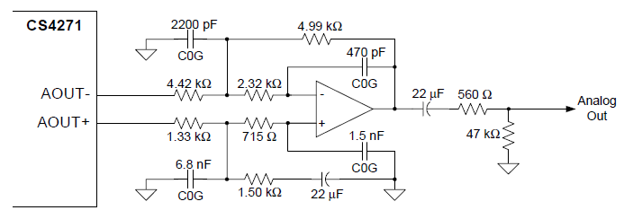
The original circuit [1]
The output circuit is based on the differential amplifier architecture, where the inverting input is subtracted from the non-inverting input.

Maximum Input Signals [1]

Hunter's PSPICE simulation of the circuit

Time Domain Output
The DC offset is not removed until after the summation of the two signals. This means the output must either be given a positive DC bias higher than 5V, or the circuit needs re-designing.
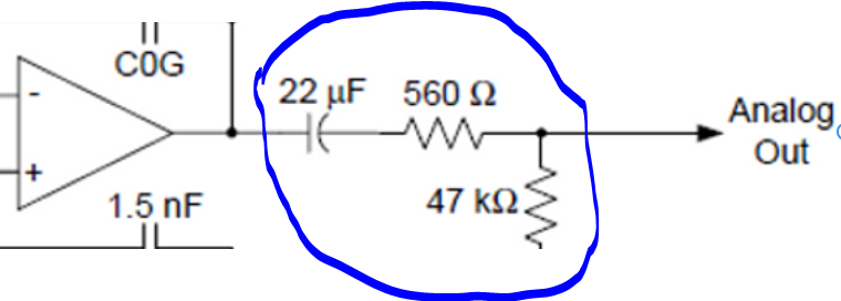
DC offset is removed by this 1st Order HPF
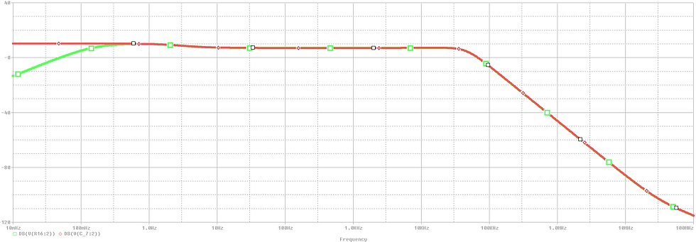
Frequency Domain Output
The suggested circuit's final output (Green) shows a Band Pass operation with Low and High cut-off's of roughly 0.086 and 50kHz respectively. The LPF is 2nd Order (12dB/Octave roll off).

Redesigned Circuit
The redesigned circuit above places 2 band-pass filters in front of the differential amp.

Time Domain Output
Above, the input signal (purple) has its DC offset removed (Red) and is summed with the second signal (Green)
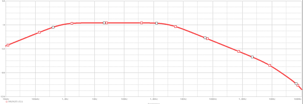
Frequency Domain Output
The filtering is accomplished by a HPF followed by a LPF, both 1st Order. Since the device is not expected to operate above 300Hz, the LPF fc is set to 3kHz. The LPF is set to 1Hz.
The differential amp provides an attenuation of about -2.5dB. This is done to keep the the Power amp from clipping at its minimum gain value of 20dB. [2]

DAC breadboard testing results at East Campus (Finish adding Tomorrow)

(Finish adding Tomorrow)

Positive input and DAC summer output
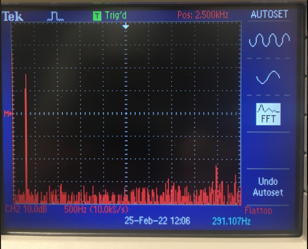
FFT of circuit output 291Hz

FFT 51.17 Hz
The team was also able to test the power supply with this circuit in order to observe and measure any issues that might arise when powering a sensitive analog circuit. The Inductors had recently been upgraded to the shielded type and the team was curious to see if any improvement in EMI and noise could be seen.
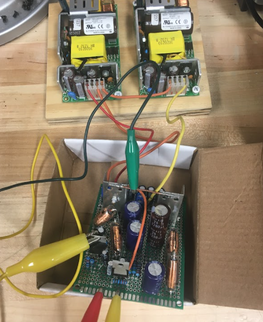

Measuring the -5V output

Noise was <20mVpp

3.3V output

Noise/Ripple on the 3.3 rail was <13mVpp!

5V supply

Again noise on the line was <13mVpp

12V supply
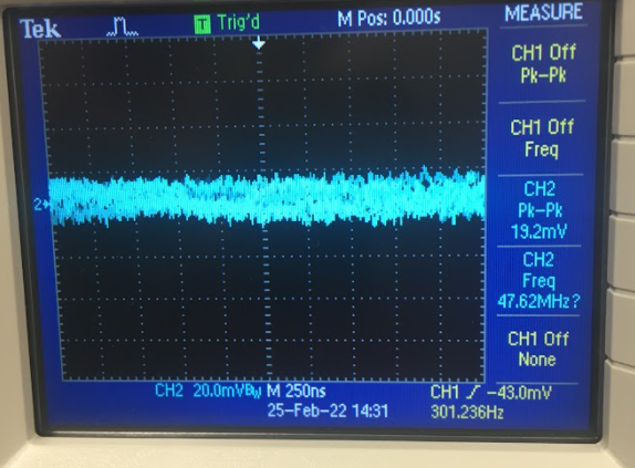
Noise was again <20mVpp
It would appear that the new inductors have drastically improved the noise/ripple performance of the power supply!
[1] Cirrus Logic, “24-Bit, 192 kHz Stereo Audio CODEC,” CS4271 datasheet, August 2005
[2] Texas Instruments, “LM1875 20W Audio Power Amplifier,” LM1875 datasheet, May 2004 [Revised May 2004].
John
This week John began the breadboard construction of the input stage of the device. He built the preamp/buffer in stages and used the PC-based Velleman Scope to take measurements along the way

Single Channel Band-Pass Filter

Bode Plot from 1-10kHz 1dB/division

Bode Plot from 1k-1MHz 5dB/division
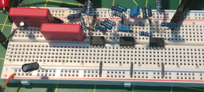
Single Channel with Gain of 2.8

1-10kHz 1dB/div
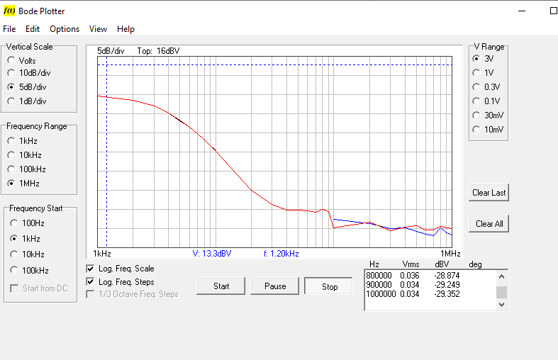
1k-1MHz 5dB/div

Single Channel with DC Offset

1-10kHz 1dB/div
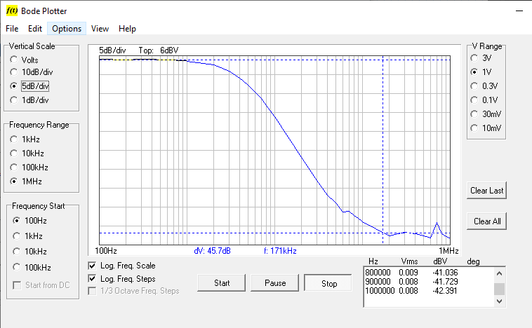
100 - 1MHz 5dB/div
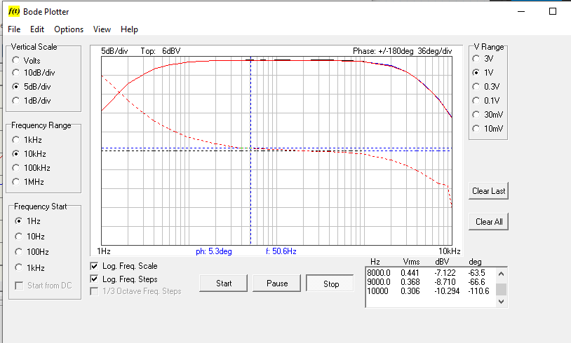
Phase Plot 5.3deg @ 50.6Hz

0.0 deg @ 302Hz
John then attempted to take a group delay measurement using a square wave function. He was unsure if the measurement was accurate and plans on using a higher quality scope to verify.

Attempt at Measuring Group Delay (appears to be ~50uS @ 50Hz)
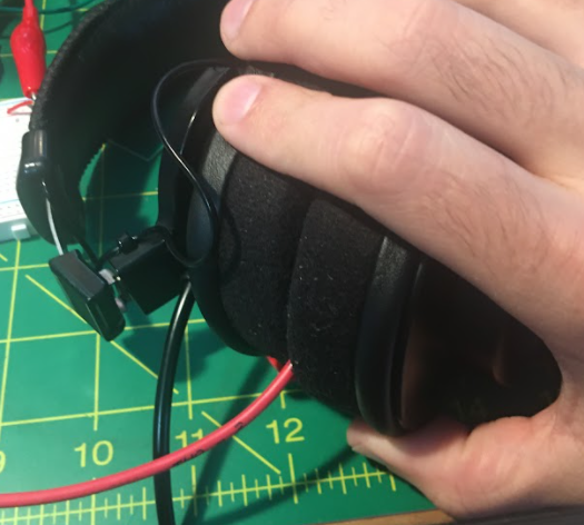
The MEMs mic was then added to verify its integration with the preamp. The mic was placed inside of a pair of headphones that played several sine functions.

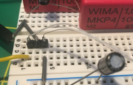
3-pin Header Breadboard Connection

Headphones closed around the mic to increase SPL
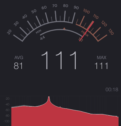
SPL inside Headphones measured with a Phone App

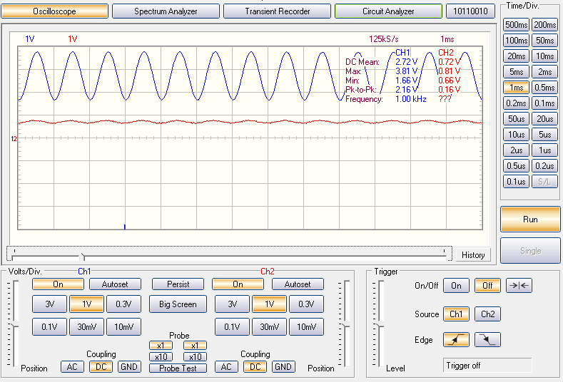
Measurement of Direct Mic output and Preamp (gain 2.8) out @~111dB SPL
The measured Mic output was much lower than expected. The Preamp gain was increased from 2.8 to 22 for a second round of testing.

Mic Outputs: Preamp gain of 22
The second MEMs mic was then measured using the same preamp and test signal
The second channel was then added and measured.


Both Preamps 1-10kHz 5dB/div

Both Preamps 1-10kHz 1dB/div

Both Preamps 1k - 1MHz 5dB/div
After both Preamps were successfully breadboarded, John used the facilities at his job on East campus to more thoroughly test the MEMs Mics.
John used an SPL meter, power supply, Tektronics Scope, and small Genelec Speaker to conduct the test. Several functions were played through the speaker. The MEMs mics and SPL meter were placed as close as possible to the speaker. By measuring both the SPL and the voltage output of the mics, John could determine the mics maximum expected outputs.
The datasheet lists a spec of 0.355 Vrms (~1Vp-p) @ 130dB SPL [1]
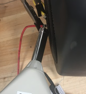
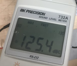
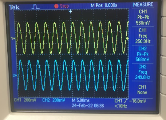

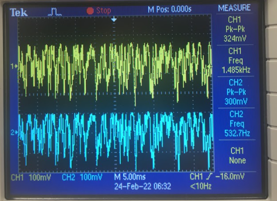
The maximum recorded voltage was measured at 568mVp-p for a 250Hz Sine wave with SPL of 125.4 dBc. The preamp gain will therefore be changed from 2.8 to:
2.8/.568 = 4.9296
rounding down to 4.9
This will allow for the capture of a cleaner signal at lower levels while still maintaining the dynamic range of the device's inputs.
It is also worth noting that the waveform outputs of each mic are identical
John also recorded the real-world test signals that will be used for to test the device. These include an AC outdoor condenser unit, Gasoline Lawnmower, Small Air Compressor, and a Table Saw.

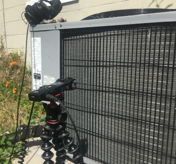
John also performed some quick spectrum analysis on the recordings using Audacity's built in analyzer. The Lawnmower show strong peaks at 100, 200, and 300 Hz

Lawnmower Spectrum Analysis
The AC Unit has a much lower Fundamental of 35 Hz with prominent a 2nd Harmonic at 70 Hz

AC Unit Spectrum Analysis
John also started breadboarding and testing the Cirrus Codec and DSP integration.
He used sigma studio to initialize the DSP and configure the correct clock ratios in order to control the CODEC. The DSP serves as the master clock in this case.
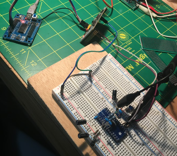
From left to right: USBi interface, DSP Eval Board, Codec Breadboard
The CODEC was able to generate the appropriate LRCLK based on the DSP mclk input!
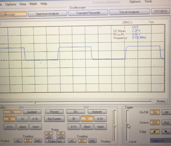
The LeftRightClock output of the ADC
LRCLK frequency represents the sample rate of the i2s datastream. 192kHz was chosen for optimal latency performance.
[1] InvenSense, “High SPL Analog Microphone with Extended Low Frequency Response,” DS-ICS-40300-00 datasheet, August 2015.
Hunter
This week Pspice simulations for the DAC output connections and Power Amplifier were tested. After reading over the CS4271 (DAC) and LM4562 (Power-Amp) data sheets and analyzing several simulations for both the DAC and the Power Amplifier separately, before connecting them together, it became clear that the schematic for the DAC's output connections in the datasheet needed to be re-designed to work efficiently. As described above, a re-design was required because the DC offset was not being removed until after the summation of the two signals coming from each of the DAC op-amps, as displayed above in the first two Pspice pictures of the team work section. [1]
The power amp did simulate as expected, when tested on its own, but when paired with the DAC’s original schematic the output gain dropped significantly. These results can be seen below for comparing the original simulation with the re-designed version. [2]
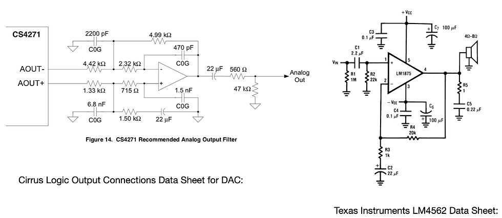

Original schematic used from Cirrus Logic datasheet (above), displaying an unexpected low output (below):
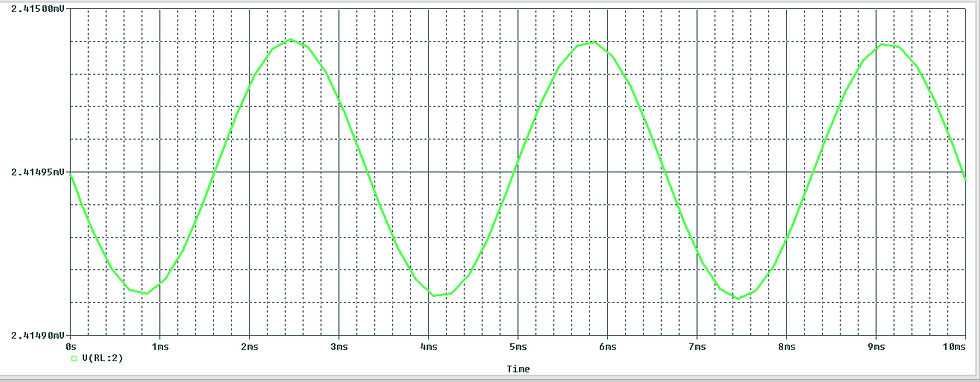
Re-designed and working DAC output connections, using three Audio Amplifiers (below):

Upon discussing this issue with my partner it became evident that the circuit needed to be modified. John applied his excellent engineering knowledge and re-designed most of the circuit (shown above) in order to achieve the desired output specifications for the DAC. The re-designed version can also be seen in the team work section above.
With the redesign of the DAC output working in the simulations we were confident to begin building it on the breadboard for testing. The team planned to meet on Thursday night, hoping for a successful night of test trials.
Thursday nights DAC breadboard testing was successful, with the results displaying the expected outputs that now match the Pspice outputs. Details of the results are explained in the team section above, as this was accomplished as a team, at the East Campus. Below, is the DAC output connections built on the breadboard and tested using a function generator and oscilloscope.


DAC output of the combined input signals (Ch1-Yellow), Function Generator (Ch2-Blue):
The power amplifier will be tested later in the week, and if results are successful, the DAC output will then be tested in conjunction with the power amplifier. Successful results of both circuits will initiate their final design of soldering them to a PCB and begin their test trials.
DAC/Power Amplifier on breadboard, testing results coming soon:
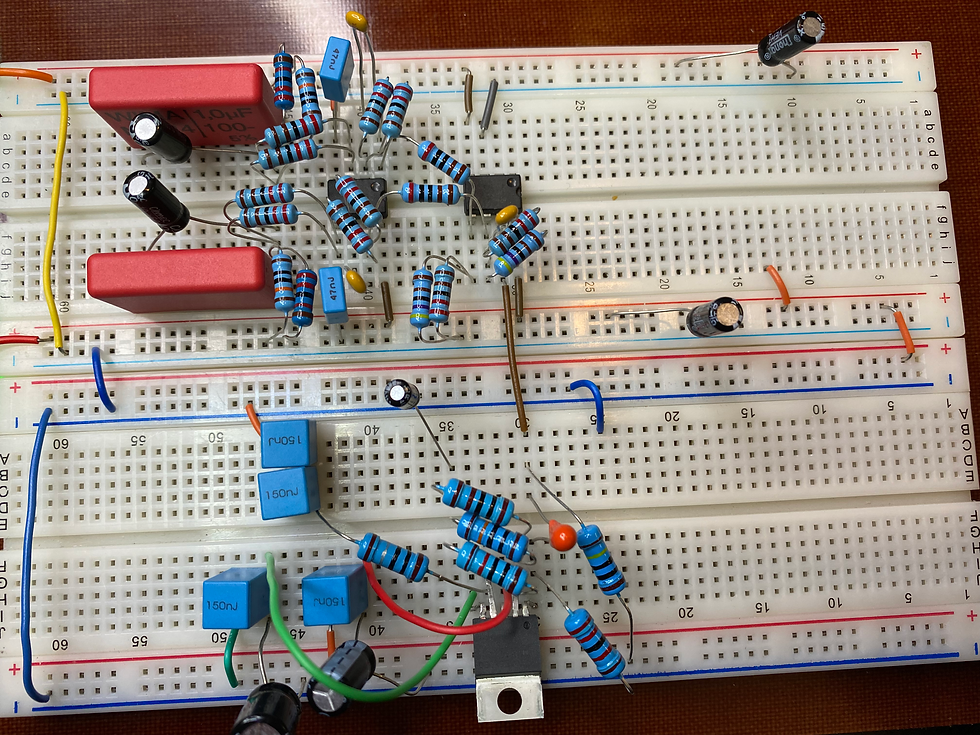
Close-up of the Power Amplifier side of breadboard:

Testing was also done with the Arduino TFT LCD by applying an electret microphone to read the analog output and see how well it works at reading the input signal, and if there are any possible limitations. A program for an oscilloscope functionality was modified and can be seen in the video below, although this seemed like it could be a nice feature to add to the UI by display the active frequencies, the coding is extensive and seems to cause a lot of lag while displaying the output signal. This program also has a moderate delay with the button response.
The idea of attempting to implement this large or a program proved to be too time intensive, but has also confirmed that the simplified/user friendly option for the TFT’s GUI to display the values of the SPL and the fundamental frequency, as originally planned for in the success criteria, will be the only goal for the remainder of Arduino testing, due to time limitations.
Updates to the website were also made to multiple pages of the Senior Design section. These sections include:
Weekly Minutes with Professor:


The Proposed Budget, Power Budget, Weekly Presentation, and the Timeline and Weekly Schedule were also added to the Design sections tab drop down menu.
References:
[1] Cirrus Logic, “24-Bit, 192 kHz Stereo Audio CODEC,” CS4271 DAC datasheet, August 2005.
[2] Texas Instruments, “LM4562 Dual High-Performance, High-fidelity Audio Operational Amplifier,” LM4562 datasheet, August 2005 [Revised December 2013].


Comments